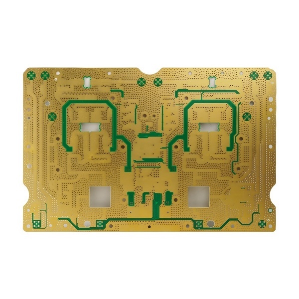
Gerber Files Printed Circuit Board PCB Fabrication for Home Appliance
♦ What's Gerber File?
A Gerber file is the standard file format used in the PCB (Printed Circuit Board) industry to describe the physical characteristics of each layer of a PCB design. Think of it as the "blueprint" or "recipe" that PCB manufacturers use to fabricate the actual board.
Here's a more detailed explanation:
-
Purpose: Gerber files tell the manufacturer precisely where to place copper (traces, pads), where to create solder mask openings, where to apply silkscreen markings (component outlines, text), and where to drill holes. Each layer of the PCB (e.g., top copper, bottom copper, top solder mask, bottom silkscreen, drill holes) is typically represented by a separate Gerber file.
-
Format: The format is an open ASCII vector format. It essentially describes shapes (like lines, arcs, circles, and polygons) using coordinates and drawing commands. It can also include aperture definitions, which define the shapes and sizes of the drawing tools (like pens or flash pads) used to create the features.
-
Evolution:
-
Standard Gerber (RS-274-D): An older version that required a separate aperture file. It's largely obsolete now.
-
Extended Gerber (RS-274X): The most common format currently. It includes the aperture definitions within the file itself, making it a complete, self-contained description of the layer. This is what most people mean when they say "Gerber file" today.
-
Gerber X2: A newer version that adds extra metadata to the files, like design attributes (pad types, component information, layer stack-up details). This helps manufacturers automate processing and perform better DFM (Design for Manufacturability) checks.
-
File Extension: Gerber files typically have extensions like .gbr, .gb, .gbo, .gtl, .txt (for drill files), or sometimes .art. The naming convention often indicates the layer (e.g., .gtl for "Gerber Top Layer", .gbl for "Gerber Bottom Layer", .gto for "Gerber Top Overlay" (silkscreen)).
-
Importance: Gerber files are the de facto standard for transferring PCB design data to manufacturers. Almost all PCB design software (EDA tools) can generate Gerber files, and all PCB fabrication houses accept them.
♦ Technical Parameters
| Item | Specification |
| Laers | 1~64 |
| Board thickness | 0.1mm-10.0mm |
| Material | FR-4,CEM-1/CEM-3,PI,High Tg,Rogers |
| Max panel size | 32"×48"(800mm×1200mm) |
| Min hole size | 0.075mm |
| Min line width | 3mil(0.075mm) |
| Surface finish | OSP,HASL,Imm Gold/Nickel/Ag, Electric gold |
| Copper thickness | 0.5-15 OZ |
| Soldermask | Green/Yellow/Black/White/Red/Blue |
| Silkscreen | Red/Yellow/Black/White |
| Min PAD | 5mil(0.13mm) |
| Inter package | Vacuum |
| Outer package | Carton |
| Outline tolerance | ±0.75mm |
| Hole tolerance | PTH:±0.05 NPTH:±0.025 |
| Certificate | UL,ISO 9001,ISO14001,IATF16949 |
| Special request | Blind hole+Gold finger + BGA |
| Material Suppilers | Shengyi, KB, Nanya, ITEQ,etc. |