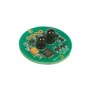
Bluetooth Speaker PCB Assembly Smart Voice Device PCBA Manufacturer
♦ What is PCB assembly?
PCB Assembly, also known as PCBA (Printed Circuit Board Assembly), is the intricate process of soldering electronic components onto a bare printed circuit board (PCB) to create a fully functional electronic circuit. This process is fundamental to the manufacturing of virtually all modern electronic devices, from smartphones and computers to medical instruments and aerospace systems.
♦ The PCB assembly process?
1. Solder Paste Printing
The first step involves applying solder paste to the bare PCB. A stencil is used to ensure that the paste is deposited only on the pads where components will be placed. The paste is a mixture of powdered solder and flux, which helps the solder melt and bond during the soldering process.
2. Component Placement
Next, electronic components such as resistors, capacitors, integrated circuits (ICs), and connectors are placed onto the PCB. This is typically done using Surface Mount Technology (SMT), where components are positioned directly onto the surface of the board using automated pick-and-place machines. These machines can place thousands of components per hour with high precision.
3. Reflow Soldering
After the components are placed, the PCB is passed through a reflow oven. This oven has multiple temperature zones that gradually heat the board to melt the solder paste, creating strong electrical and mechanical connections between the components and the PCB. The temperature profile is carefully controlled to prevent thermal shock and ensure uniform soldering.
4. Inspection and Quality Control
Post-soldering, the assembled PCB undergoes rigorous inspection to detect any defects. Common inspection methods include:
Automated Optical Inspection (AOI): Uses high-resolution cameras and AI to detect misalignments, missing components, and solder defects.
X-ray Inspection: Used to inspect hidden solder joints, especially for Ball Grid Arrays (BGAs) and other complex components.
In-Circuit Testing (ICT): Checks the electrical performance of the assembled board to ensure it functions as intended.
5. Through-Hole Technology (THT)
For components that require stronger mechanical bonds or are not suitable for SMT, Through-Hole Technology is used. Component leads are inserted into drilled holes on the PCB and soldered on the opposite side. This can be done manually or using automated wave soldering machines.
6. Final Assembly and Testing
Once all components are soldered and inspected, the PCB may undergo additional processes such as conformal coating for protection against environmental factors. Functional testing is then performed to verify that the assembled PCB operates correctly under real-world conditions.
♦ DQS's PCB Assembly Capability
| Item | Normal | Special |
| SMT Assembly | PCB(for SMT) specification | Length and Width( L* W) | Minimum | L≥3mm, W≥3mm | L<2mm |
| Maximum | L≤800mm, W≤460mm | L > 1200mm, W>500mm |
| Thickness( T) | Thinnest | 0.2mm | T<0.1mm |
| Thickest | 4 mm | T>4.5mm |
| SMT components specification | Outline Dimension | Min size | 0201(0.6mm*0.3mm) | 01005(0.3mm*0.2mm) |
| Max size | 200 * 125 | 200 * 125 |
| component thickness | T≤15mm | 6.5mm<T≤15mm |
| QFP,SOP,SOJ (multi pins) | Min pin space | 0.4mm | 0.3mm≤Pitch<0.4mm |
| CSP/ BGA | Min ball space | 0.5mm | 0.3mm≤Pitch<0.5mm |
| DIP Assembly | PCB specification | Length and Width ( L* W) | Minimum | L≥50mm, W≥30mm | L<50mm |
| Maximum | L≤1200mm, W≤450mm | L≥1200mm, W≥500mm |
| Thickness( T) | Thinnest | 0.8mm | T<0.8mm |
| Thickest | 3.5mm | T>2mm |
♦ One-Stop Electronic Manufacturing Including
| PCB Prototype | Quick Turn PCB | Single-Sided PCB | Double-Sided PCB | Multilayer PCB | Rigid PCB |
| Flexible PCB | Rigid-Flex PCB | Rigid-Flex PCB | Aluminum PCB | Metal Core PCB | Thick Copper PCB |
| HDI PCB | BGA PCB | High TG PCB | PCB Stencil | Impedance Control PCB | PCB Assembly |
| High-Frequency PCB | Bluetooth Circuit Board | Automotive PCB | USB Circuit Board | Halogen-Free PCB | Antenna PCB |
♦ Core Competencies of DQS PCB Assembly
| SMT | 
| DIP |
|
- 13 automatic high-speed SMT line
- 5 million points / day
- FPC/Double sided mounted
- Automatic conformal coating
| - 4 DIP line
- Post-soldering700,000 points/day
- Professional DIP plug-in team
|
| SMT Technology | | PCBA OEM |
- Min package: 01005
- Min pin: 0.3mm
- Min BGA pitch: 0.3 mm
|
- Full turnkey PCB assembly
- Partial turnkey PCB assembly
|