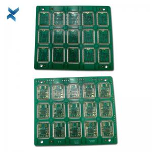
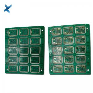
China Electronic Products PCB/PCBA Supplier Multilayer PCBA PCB Assembly Service Supplier
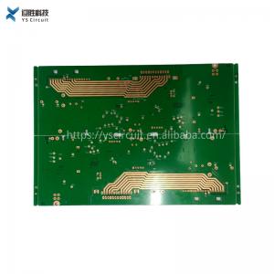
What is Multilayer PCBs
Multilayer Printed Circuit Board, It is a type of PCB which comes with a combination of single sided PCB and double sided PCB.
It features layers more than double sided PCB.
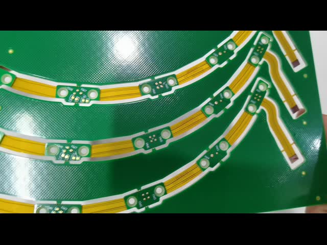
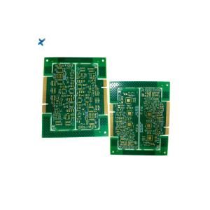
PCB Sideplating
Sideplating is the metalization of the board edge in the PCB filed.
Edge plating, Border plated, plated contour, side metal, these words can also be used to describe the same function.
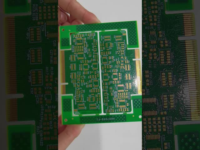
Half-cut Castellated Holes
Castellations are plated through holes or vias located in the edges of a printed circuit board.
Are indentations created in the form of semi-plated holes on the edges of the PCB boards.
These half holes serve as pads intended to create a link between the module board and the board that it will be soldered onto.
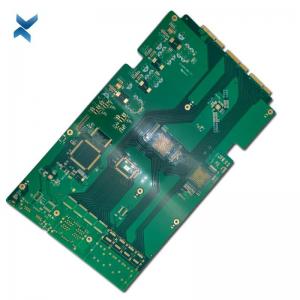
Parameters
- Layers: 10L multilayer pcb
- Board Thinkness:2.0mm
- Base Material:S1000-2 High tg
- Min Holes:0.2mm
- Minimum Line Width/Clearance:0.25mm/0.25mm
- Minimum Clearance between Inner Layer PTH to Line: 0.2mm
- Size:250.6mm×180.5mm
- Aspect Ratio:10 : 1
- Surface treatment:ENIG+ Selective hard gold
- Process characteristics: High tg, Sideplating, Selective hard gold, Half-cut Castellated Holes
- Applications: Wi-Fi modules
| YS Multilayer PCB manufacturing capabilities overview |
| Feature | capabilities |
| Layer Count | 3-60L |
| Available Multilayer PCB Technology | Through hole with Aspect Ratio 16:1 |
| buried and blind via |
| Hybrid | High Frequency Material such as RO4350B and FR4 Mix etc. |
| High Speed Material such as M7NE and FR4 Mix etc. |
| Thickness | 0.3mm-8mm |
| Minimum line Width and Space | 0.05mm/0.05mm(2mil/2mil) |
| BGA PITCH | 0.35mm |
| Min mechanical Drilled Size | 0.15mm(6mil) |
| Aspect Ratio for through hole | 16:1 |
| Surface Finish | HASL, Lead free HASL,ENIG,Immersion Tin, OSP, Immersion Silver, Gold Finger, Electroplating Hard Gold, Selective OSP,ENEPIG.etc. |
| Via Fill Option | The via is plated and filled with either conductive or non-conductive epoxy then capped and plated over(VIPPO) |
| Copper filled, silver filled |
| Registration | ±4mil |
| Solder Mask | Green, Red, Yellow, Blue, White, Black, Purple, Matte Black, Matte green.etc. |

FQA
1. What is hard gold in PCB?
The Hard Gold surface finish, also known as Hard Electrolytic Gold, is composed of a layer of gold with added hardeners for increased durability, plated over a barrier coat of nickel using an electrolytic process.
2. What is hard gold plating?
Hard gold plating is a gold electrodeposit that has been alloyed with another element to alter the grain structure of the gold to achieve a harder deposit with a more refined grain structure.
The most common alloying elements used in hard gold plating are cobalt, nickel or iron.
3. What is the difference between Enig and hard gold?
ENIG plating is much softer than hard gold plating.
Grain sizes are about 60 times larger with ENIG plating, and hardness runs between 20 and 100 HK25.
ENIG plating holds up well at only 35 grams of contact force or less, and ENIG plating typically lasts for fewer cycles than hard plating.
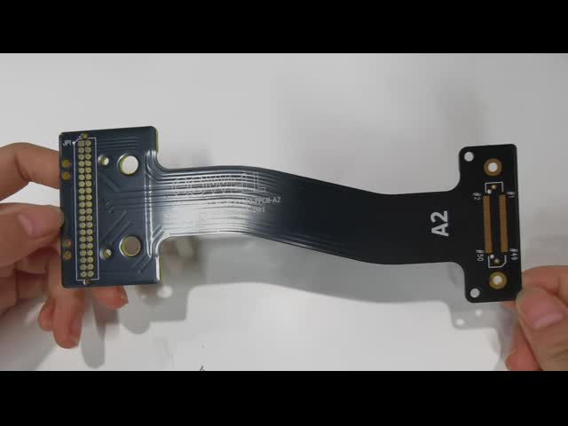
A popular trend among manufacturers is board-to-board soldering.
This technique allows companies to produce integrated modules (often containing dozens of parts) on a single board that can be built into another assembly during production.
One easy way to produce a PCB that is destined to be mounted to another PCB is to create castellated mounting holes.
These are also known as "castellated vias" or "castellations."